Hi guys
Can someone tell me about the makerbuino circuit scematics:
- What are SJ1 and SJ2 in the schematics? I cant find anywhere on the WWW where someone uses it in schematics.
- Why are all the breakouts referred to as JPs? (jumpers?)
Hi guys
Can someone tell me about the makerbuino circuit scematics:
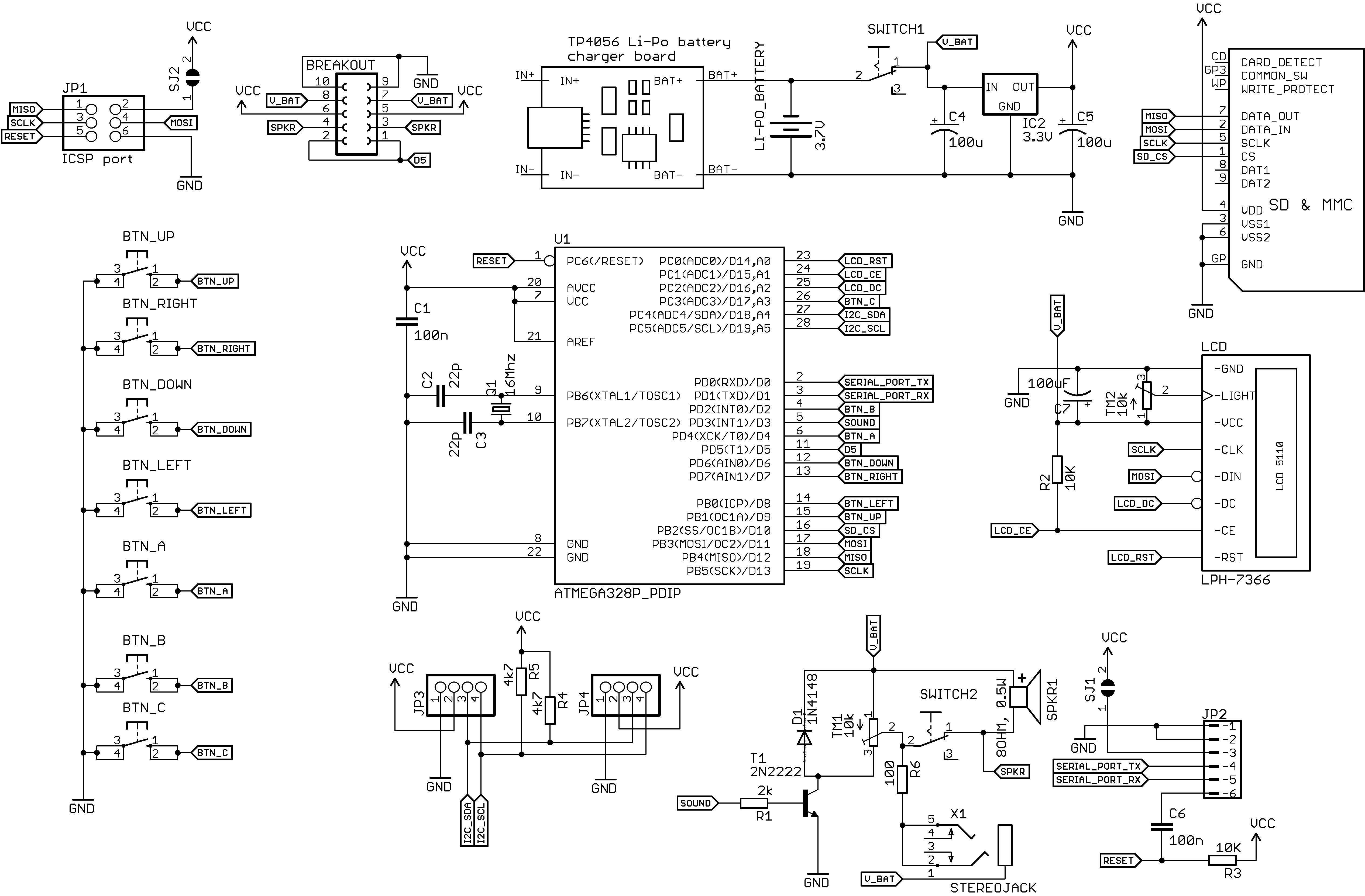
Yres, this schematic come from the PDF here: http://gamebuino.com/wiki/index.php?title=Hardware
(section schematics) and you will find the list of components at the section Bill Of Materials
SJ1 and SJ2 are solder jumpers. It is like for configuration or debugging of the board after manufacturing.
JP is just the defaut name in Eagle CAD software for this kind of component…
Thanks guys. So for SJ1/SJ2.
Does it mean that if you want to use it you should ‘manually’ do a soldered bridge to VCC or is it already on the board?
Is the two semi circles suggesting that the connection is broken? Or that it connects to VCC through the jumper (probably more logical)
Hey @Kakpraatjies!
Looks like those two solder jumpers are for enabling or disabling the power over the ICSP and serial ports, and probably come desoldered for safety. If you want to enable those, yes, you should make a little blob of solder between the two points. That will connect the pins to VCC.
Of course, making this will enable you to power little boards from the two ports, but be careful of what you power from the console, since I’m pretty sure a short-circuit will be very bad for the little makerbuino 
In brief: don’t touch this unless you know what you are doing.