Someone can explain me how read electronic schematics?
Depends on what you want to know  is this your first time reading schematics?
yes i m newbie in electronic
Alright I’ll gather some information for you later today, stay tuned
1 Like
First of all there is a difference between reading a schematic and understanding a schematic. To understand it you’ll need some knowledge of the basic electronic components and how they work together in circuits. I think I’ll split this up into a couple of posts as it’s a lot of stuff and it will take me a lot of time to explain everything.
Let’s start with the basics of a schematic.
The lines between the different parts are representing the connections. As you can see in the following picture there are two different kinds of crossing lines. The ones without a dot and the ones with a dot.

If there are two lines crossing each other and there is no dot (like the blue marked example) there is no connection between those lines (or signals). If there are two lines crossing each other and there is a black dot then those lines (or signals) are connected. Check the arrows to see how the signals are flowing. This is of course a pretty brief example, not the actual flow of current. And please excuse my poorly drawn arrows and circles 
The next thing are those flag like symbols. They are called Ports. You’ll use ports to avoid drawing a full connection line all over the schematic as this will make your schematic really messy. And this is where you’ll use those ports. Ports with the same name are sharing the same signal as you can see in the following picture.

Same goes for the voltages. Take a look at the next picture.
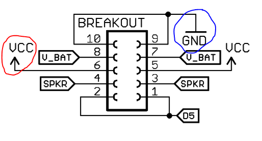
The marked symbols work like ports but they look different. Those symbols can differ a little bit, depending on which software you use to create your schematics. The upward arrow of VCC could also be a circle and the GND symbol could look like a three legged fork (for example). As i said those work like ports. This makes it very easy to clean up your schematic as you won’t need to connect every part to the voltage regulator or power supply.
The last part of this post will cover the different voltages/signals.
Both, VDD and VCC, are describing a positive voltage like 3.3V or 5V (common values for many circuits).
The MAKERbuino runs with 3.3V after the voltage regulator.
On the other side VEE and VSS are describing a negative voltage but they are often identical with GND (ground).
GND stands for ground and you can think of it like it has 0V all the time. This is because the voltage is a difference in electric potential energy between two points. So if you’re measuring voltage with a multimeter you’re basically measuring the difference between a measurement point compared to another point (mostly GND). You won’t need a negative voltage most of the time if you’re hacking your MAKERbuino.
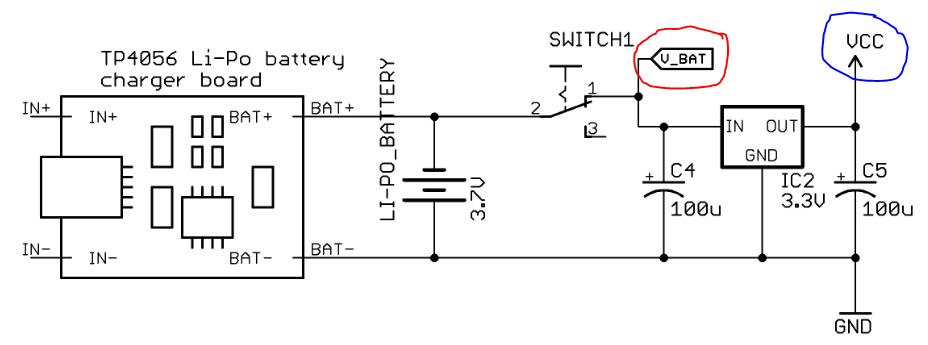
And then the MAKERbuino has a VBAT. This is simply the voltage supplied by the battery. It’s an 3.7V lithium-polymer battery. The difference between VBAT and VDD/VCC is that the voltage from VBAT is unregulated and therefore not constant. This is why the MAKERbuino needs a voltage regulator (IC2 if you look at the schematic). It provides 3.3V constantly which is important when it comes to supplying IC’s.
Everything inside your MAKERbuino uses the regulated VCC/VDD except for three things: The display, the Stereojack and the breakout pins.
As you can see in the picture the unregulated VBAT is marked with a red “circle” and the regulated VCC is marked with a blue “circle”.
I think the next post will be about the basic components of the schematic like resistors, potentiometers, buttons and switches. If you have a question regarding anything covered in this post just let me know
4 Likes
Very good! Thanks

I will study more!
First of all I’m sorry that it took me so long to write the next part. The company I’m working for had a lot of work in the last couple of months.
Now I’m going to cover the connectors, buttons and switches. I know I said that I wanted to cover the resistors and potentiometers in this post too. But I think it’s better to cover those components first, because there is a lot of explanaition needed when it comes down to electronical components. Especially if they change the behaviour of the circuit. But I already started writing the third part which will cover resistors and potentiometers.
So Let’s start with the connectors, because they’re very easy to understand. There is not much to say about connectors in schematics. Everything should be pretty selfexplanatory as there are only a couple of numbered pins. So let me tell you something about connectors in general.
Connectors are coming in various different shapes and sizes, but they all work in the same way. After soldering them you’re able to grab the connected signals at the determined pins. It doesn’t matter if the connector is a male one or a female one. The MAKERbuino mostly uses male ones. The only female connector is J2 and it’s used to establish the serial connection.
As you can see you can even use ports to connect the signals to the pins of a connector. Take a look at part 1 if you’ve forgotten how ports are working. If you take a look at your MAKERbuino PCB you’ll see that the signals that are routed to the connectors are named. This is a pretty good practise as it’s very easy for you to remember which signal is connected to a certain pin of the connector. This way you won’t need to look at your schematic every time you want to grab a certain signal.
If you’re working with your MAKERbuino or with Arduino/Raspberry Pi boards you’ll mostly encounter simple pin headers. These are the easiest way to connect something to those boards or your own creation. They’re often used for jumpers aswell. But you’ll need to be very careful if you’re using pin headers as a connector! They don’t offer a good anti-reversing protection. So it’s very easy to connect pin headers wrong. This way you could end up creating a short circuit by connecting VCC to GND or something like that. A short circuit can cause severe damage to the involved circuits.
Fortunately there are connectors which prevent you from inserting the corresponding plug in a wrong way. The MAKERbuino uses one of them. Take a look at the I2C-Headers JP3 and JP4. The housing offers an anti-reversing protection. It’s the white “nose” like thingy on the bottom. Another example is a boxed pin header. The connector has a notch on one side of the box and the corresponding plug offers a nose on the same side.
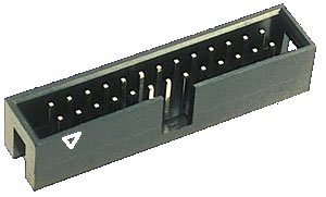
(image from wikipedia.com)
I think this should cover almost everything you’ll need to know about connectors. If there’s something still unclear just ask me right away.
Let’s move on to the buttons. There are a lot of different types of buttons. The MAKERbuino uses those big square-shaped clicky push-buttons. They require quite a lot of force to operate compared to other buttons. Many Makers are using smaller push-buttons which require less force to operate. They’re very common and very cheap. But there are also bigger buttons with pilot lights build in and stuff like that. There are also different ways to connect a button to your circuit. The buttons of the MAKERbuino are soldered directly to the PCB using THT (Through Hole Technology). Other buttons are soldered directly to the PCB using SMT (Surface-Mounting Technology). You may know the term SMD (Surface-Mounted Device). But there are also buttons which are connected to your circuit using wires because you can mount them in a casing.
Buttons can function in two different ways. There are NO buttons (NO = Normally Open) and NC buttons (NC = Normally Closed). You’ll mostly encounter NO buttons. The buttons of the MAKERbuino are NO buttons too.
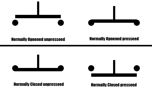
You might have guessed what the difference is, but I’ll explain it anyway. If you’re pushing a NO button you’re establishing a connection between the pins of the button. And if you’re pushing a NC button you’re disrupting an existing connection between the pins of the button.
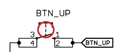
Let’s see how the buttons of the MAKERbuino are working. As I said those are NO buttons. They are open so there is no connection between the pins 1+2 and 3+4. Take a look at the following picture:
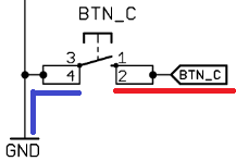
I’ve marked the different signals on each side of the button. The blue line is GND and the red line is VCC. Why is there a VCC signal on the right side you ask? That’s something I’ll cover in the next part as it has something to do with resistors. I’ll definetly cover those in the next post as resistors are basic components of a circuit. But just accept the fact that there is a VCC signal on the right side for now.
But how does the MAKERbuino recognise the push of a button? That’s very easy. Just take a look at the following picture:
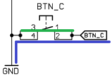
Imagine you’ve just pushed the button. You’ve closed the bridge between the pins 1+2 and 3+4. Now there’s a connection and the signal is changing to GND on the right side of the button. As you can see there is another port-flag right next to the button which is named “BTN_C”. Take a look at the ATMEGA328P_PDIP named “U1” in the schematic. You’ll see that there is a corresponding port-flag. This means that the GND signal “reached” pin 26 of the ATMEGA328. The Gamebuino library recognises the GND (or LOW) signal as a pushed button.
If you release the button it changes back to its original state (open, because it’s a NO button) and the connection between the pins is disrupted again. Resulting in a GND signal on the left side and a VCC signal on the right side of the button. And that’s the difference between buttons and switches: Switches won’t change back to their original state after you release them.
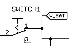
But how to determine if the symbol in the schematic is a button or a switch? If you look at the schematic of the MAKERbuino it’s quite easy because they’ve got three pins aligned in different directions.
But there is another small detail which you may already saw:
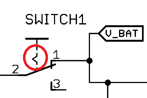
If there is a “nose” it’s a switch. If there is a straight line (like in the following picture) it’s a button.
I really hope it helps to understand the schmatic of the MAKERbuino! As I said I’m already writing part 3 so stay tuned! Just ask me if there is something unclear
1 Like